DOL-HDR, HDR, and Dolby Vision are high-dynamic range (HDR) imaging types. HDR imaging captures and displays images with a broader range of brightness and colors than standard dynamic range (SDR) imaging. This can make images look more realistic and immersive.
Comparison table of SDR, HDR, and Dolby Vision:
Feature
SDR
HDR
Dolby Vision
Dynamic range
Limited
Wide
Wider
Color gamut
sRGB
DCI-P3
Rec. 2020
Bit depth
8-bit
10-bit
12-bit
Metadata
Static
Static or dynamic
Dynamic
Compatibility
Widespread
Limited
Widening
Price
Affordable
More expensive
Most expensive
SDR stands for Standard Dynamic Range. It is the most common type of video format, and it is what most people are used to seeing. HDR stands for High Dynamic Range. It offers a broader range of colors and brightness than SDR, making images look more realistic and immersive. Dolby Vision is a type of HDR that offers an even wider color gamut and brightness than HDR. It is also more dynamic, which can adjust the image’s brightness and contrast scene by scene.
HDR and Dolby Vision offer several benefits over SDR, including:
More realistic and immersive images
Greater detail in both bright and dark areas of the image
Improved contrast and color
Reduced glare and blooming
However, HDR and Dolby Vision also require more powerful hardware to display correctly. Most TVs and monitors do not support HDR or Dolby Vision, and even those that do may be unable to display it at its full potential.
DOL-HDR stands for Digital Overlap High Dynamic Range. It is a type of HDR imaging that captures multiple exposures of an image simultaneously rather than one at a time. This allows smoother transitions between bright and dark areas in the image and can help reduce noise and artifacts.
HDR stands for High Dynamic Range. It is a type of imaging that captures a broader range of brightness and colors than standard dynamic range (SDR) imaging. This can make images look more realistic and immersive.
Dolby Vision is a type of HDR imaging developed by Dolby Laboratories. It is a proprietary tech licensed by Dolby that offers a broader range of colors and brightness than HDR, and it is also more dynamic, meaning that it can adjust the image’s brightness and contrast scene by scene.
These three technologies offer improved image quality over standard dynamic range (SDR) imaging. However, there are some key differences between them.
DOL-HDR is the most affordable option but offers the narrowest range of colors and brightness.
HDR is a good middle ground between DOL-HDR and Dolby Vision and is more widely compatible.
Dolby Vision offers the broadest range of colors and brightness and is more dynamic than HDR. However, it is also the most expensive option.
The best type of HDR imaging for you will depend on your budget and needs. Dolby Vision is the way to go if you want the best image quality.
However, if you are on a budget or your hardware does not support Dolby Vision, then HDR is a good option. And if you are on a tight budget and your hardware does not support HDR, then DOL-HDR is a good choice.
Some of the most popular DOL-HDR hardware sensors include:
These sensors offer a wide range of features and benefits, including:
High resolution
Wide dynamic range
Fast autofocus
Low-light performance
Here are some additional information about these technologies:
DOL-HDR is a relatively new technology quickly becoming more common in smartphones and other consumer cameras. It is a powerful tool that can help improve your image quality, regardless of the lighting conditions.
HDR has been around for a few years now, and it is becoming more widely supported by TVs and other devices. It offers a noticeable improvement in image quality over SDR, and it is a good option for those who want to improve the look of their movies and TV shows.
Dolby Vision is the newest and most advanced HDR technology. It offers the broadest range of colors and brightness and is more dynamic than HDR. However, it is also the most expensive option and is not as widely supported as HDR.
Dolby Vision is the way to go if you want the best image quality. However, if you are on a budget or your hardware does not support Dolby Vision, then HDR is a good option. And if you are on a tight budget and your hardware does not support HDR, then DOL-HDR is a good choice.
Comparison: DOL-HDR vs HDR vs Dolby Vision
Here is a comparison of DOL-HDR, HDR, and Dolby Vision:
Feature
DOL-HDR
HDR
Dolby Vision
Dynamic range
Wide
Wider
Widest
Color gamut
Wide
Wider
Widest
Bit depth
10-bit
10-bit
12-bit
Metadata
Static
Static or dynamic
Dynamic
Compatibility
Limited
Widespread
Widening
Price
Affordable
More expensive
Most expensive
Conclusion
DOL-HDR, HDR, and Dolby Vision are all types of HDR imaging that can offer improved image quality over standard dynamic range (SDR) imaging. Dolby Vision offers the widest range of colors and brightness and is more dynamic than HDR. However, it is also the most expensive option. HDR is a good middle ground between DOL-HDR and Dolby Vision and is more widely compatible. DOL-HDR is the most affordable option but offers the narrowest range of colors and brightness.
The best type of HDR imaging for you will depend on your budget and needs. Dolby Vision is the way to go if you want the best image quality. However, if you are on a budget or your hardware does not support Dolby Vision, then HDR is a good option. And if you are on a tight budget and your hardware does not support HDR, then DOL-HDR is a good choice.
Introducing the Sony IMX 766 and IMX 890 camera sensors: These cutting-edge sensors are packed with features that will take your photography and videography to the next level. With a larger sensor size, more megapixels, and improved low-light performance, the IMX 766 and IMX 890 sensors will surely deliver stunning images in any lighting condition.
Here are just a few of the features that make the IMX 766 vs. IMX 890 sensors unique:
Large sensor size: The IMX 766 and IMX 890 sensors have a larger sensor size than previous generations, which means they can capture more light and detail. This is especially beneficial for low-light photography and videography.
More megapixels: The IMX 766 and IMX 890 sensors have more megapixels than previous generations, so you can crop your images more and still get great results. This is also beneficial for printing large photos.
Improved low-light performance: The IMX 766 and IMX 890 sensors have improved low-light performance, so you can take sharper and more detailed photos in low-light conditions. This is perfect for shooting at night or in dimly lit environments.
Fast autofocus: The IMX 766 and IMX 890 sensors have fast autofocus, so you can easily capture moving subjects. This is perfect for shooting sports, action, or wildlife photography.
Video recording: The IMX 766 and IMX 890 sensors can record video in 4K resolution at 60 frames per second, perfect for creating high-quality videos.
Comparison Table: Sony IMX 766 vs IMX 890 camera sensors:
Feature
IMX 766
IMX 890
Sensor size
1/1.56 inches
1/1.3 inches
Pixel size
1.0μm
1.22μm
Megapixels
50MP
50MP
ISO range
100-51200
100-102400
Dynamic range
12.5 stops
15 stops
Autofocus
Phase detection and contrast detection
Phase detection and contrast detection
Image stabilization
OIS
OIS
Video recording
8K@30fps, 4K@120fps, 1080p@240fps
8K@30fps, 4K@120fps, 1080p@240fps
Other features
DOL-HDR, Eye AF, Real-time tracking
DOL-HDR, Eye AF, Real-time tracking
Price
$15-$20
$25-$30
As you can see, the IMX 890 has a slightly larger sensor size, larger pixel size, higher dynamic range, and a more comprehensive range of video recording features. It also costs slightly more than the IMX 766.
Ultimately, the best camera sensor for you will depend on your needs and budget. If you are looking for the best possible image quality, the IMX 890 is the better choice. However, the IMX 766 is still a great option if you are on a budget.
Sensor size
The IMX 890 has a slightly larger sensor size than the IMX 766. This means it can capture more light, improving image quality in low-light conditions.
Pixel size
The IMX 890 also has a larger pixel size than the IMX 766. Each pixel can capture more light, improving image quality in low-light conditions.
Dynamic range
The IMX 890 has a higher dynamic range than the IMX 766. This means it can capture a broader range of brightness levels in a single image, improving image quality in scenes with much contrast.
Autofocus
The IMX 766 and IMX 890 have phase and contrast detection autofocus. This means they can quickly and accurately focus on subjects, even in low-light conditions.
Image stabilization
The IMX 766 and IMX 890 have optical image stabilization (OIS). This helps to reduce camera shake, which can lead to sharper images.
Video recording
The IMX 766 and IMX 890 can record 8K video at 30fps. However, the IMX 890 can also record 4K video at 120fps, while the IMX 766 is limited to 4K video at 60fps.
Other features
The IMX 766 and IMX 890 have several other features, such as DOL-HDR, Eye AF, and Real-time tracking. These features can help to improve the quality of your images and videos.
Overall
The IMX 890 is a slightly better camera sensor than the IMX 766. It has a larger sensor size, pixel size, higher dynamic range, and broader video recording features. However, it is also slightly more expensive.
Ultimately, the best camera sensor for you will depend on your needs and budget. If you are looking for the best possible image quality, the IMX 890 is the better choice. However, the IMX 766 is still a great option if you are on a budget.
Here are some phones that use the Sony IMX 766 and IMX 890 camera sensors:
Phones with Sony IMX 766
OnePlus 10 Pro
Realme GT Neo 3
Oppo Reno 7 Pro
Xiaomi 12 Pro
Poco F4 GT
Motorola Edge 30 Pro
iQOO 9 Pro
Vivo X70 Pro+
OnePlus 9RT
Realme GT 2 Pro
Phones with Sony IMX 890
Realme GT Neo 3T
Oppo Reno 9 Pro+
Xiaomi 12S Pro
Redmi K50 Pro
Motorola Edge 30 Ultra
These are just a few phones that use the Sony IMX 766 and IMX 890 camera sensors. If you are looking for a phone with a great camera, these are some of the best options.
Conclusion
The Sony IMX 766 and IMX 890 sensors are the perfect choice for photographers and videographers who demand the best image quality. With their large sensor size, more megapixels, and improved low-light performance, these sensors will surely deliver stunning images in any lighting condition.
If you are looking for a camera sensor that can take your photography and videography to the next level, then the Sony IMX 766 and IMX 890 sensors are the perfect choice.
The Sigma 30 mm f/1.4 DC DN Contemporary Lens is a great all-around lens for APS-C mirrorless cameras. However, several other great lenses are available that offer similar features and performance.
These alternatives include the Sony 35 mm f/1.8 OSS Lens, the Tamron 30 mm f/1.4 Di III OSD M1:2 Lens, and the Zeiss Touit 32 mm f/1.8 Lens. Each of these lenses has its strengths and weaknesses, so choosing the one best suited for your needs is essential.
The Sony FE 35mm f/1.8 is an excellent option for those who want a slightly wider field of view. It’s also slightly sharper than the Sigma lens and weather-sealed.
The Panasonic Lumix S 35mm f/1.8 is another excellent option for those who want a slightly wider field of view. It’s also slightly sharper than the Sigma lens and has a focus clutch for quick and easy manual focus.
The Samyang AF 35mm f/1.8 FE is an excellent option for those who want a more affordable lens. It’s not as sharp as the Sigma lens, but it’s still a good option for those on a budget.
The Meike 35mm f/1.7 II is another excellent option for those on a budget. It’s not as sharp as the Sigma lens, but it’s still a good option for those who want a wide-aperture lens for a low price.
Ultimately, the best lens for you will depend on your individual needs and budget. If you want the best possible image quality and don’t mind spending more, the Sigma 30mm f/1.4 DC DN Contemporary Lens is a great option. If you’re on a budget, the Sony FE 35mm f/1.8, Panasonic Lumix S 35mm f/1.8, Samyang AF 35mm f/1.8 FE, or Meike 35mm f/1.7 II are all great choices.
Tabular comparison of the above lenses: Sigma 30 mm f/1.4 DC DN Contemporary Lens alternatives:
As you can see, there are a few different factors to consider when choosing a lens. The most important factor is probably the price. The Meike 35mm f/1.7 II is an excellent option if you’re on a budget.
If you can afford to spend a little more, the Sigma 30mm f/1.4 DC DN Contemporary Lens is an excellent choice for those who want the best image quality. The Sony FE 35mm f/1.8 is a perfect option for weather-sealed lenses. And if you want a lens with a focus clutch, the Panasonic Lumix S 35mm f/1.8 is a great choice.
Ultimately, the best lens for you will depend on your individual needs and budget.
Conclusion
When choosing a lens, there are a few factors to consider, such as price, image quality, weather-sealing, and focus features. The best lens for you will depend on your individual needs and budget.
The Meike 35mm f/1.7 II is an excellent option if you are on a budget. It is a sharp and affordable lens that is perfect for everyday photography.
If you can afford to spend a little more, the Sigma 30mm f/1.4 DC DN Contemporary Lens is an excellent choice for those who want the best image quality. It is a fast and sharp lens that is perfect for low-light photography.
The Sony FE 35mm f/1.8 is an excellent option for weather-sealed lenses. It is a well-built lens that is perfect for shooting in all weather conditions.
And if you want a lens with a focus clutch, the Panasonic Lumix S 35mm f/1.8 is a great choice. It is a fast and precise lens that is perfect for videography.
Ultimately, the best lens for you will depend on your individual needs and budget. By considering the factors above, you can choose the right lens for you.
Atomos Ninja V, Shogun Connect, and Ninja V+ are powerful monitor recorders that can record high-quality video from your camera. However, some key differences may make one a better choice for you than the others.
Here is a tabular comparison of Atomos Nina V vs Shogun Connect vs Ninja V+:
As you can see, the Atomos Ninja V, Shogun Connect, and Ninja V+ are all powerful monitor recorders that offer a variety of features and capabilities. The best choice for you will depend on your needs and budget.
The Atomos Ninja V is the most affordable of the three options, and it’s an excellent choice for beginners or those who don’t need all the bells and whistles. It can record up to 4K UHD video at 60fps and has a built-in 5-inch touchscreen display. It also supports a variety of codecs, including ProRes and DNxHR.
The Atomos Shogun Connect is a more powerful option than the Ninja V and is a good choice for intermediate or advanced users. It can record up to 8K ProRes RAW video at 30fps and has a built-in 7-inch touchscreen display. It also supports a broader range of codecs than the Ninja V, including Blackmagic RAW and REDCODE RAW.
The Atomos Ninja V+ is the most powerful of the three options, and it’s a good choice for professionals or those who need the absolute best image quality. It can record up to 8K ProRes RAW video at 60fps and has a built-in 5.5-inch touchscreen display. It also supports a broader range of codecs than the Ninja V, including Blackmagic RAW and REDCODE RAW.
List of compatible devices for the Atomos Ninja V, Shogun Connect, and Ninja V+:
This is just a list of some of the compatible devices. For a complete list, please visit the Atomos website.
Limitations: Atomos Nina V vs Shogun Connect vs Ninja V+
Atomos Ninja V
Can only record up to 4K UHD video at 60fps
It does not support Blackmagic RAW or REDCODE RAW
It does not have as many features as the Shogun Connect or Ninja V+
Atomos Shogun Connect
More expensive than the Ninja V
Larger and heavier than the Ninja V
Requires an external battery to operate
Atomos Ninja V+
Most expensive of the three options
It does not have as many features as the Shogun Connect
Requires an external battery to operate
As you can see, each Atomos monitor recorder has its limitations. The best choice for you will depend on your needs and budget.
Which one should you choose?
The Atomos Ninja V, Shogun Connect, and Ninja V+ are all high-end external recorders that can be used to record high-quality videos from various sources. The Ninja V is the most affordable option, but it has fewer features than the other two recorders. The Shogun Connect is the most expensive option but has the most features. The Ninja V+ is a good middle-ground between the Ninja V and Shogun Connect. It has more features than the Ninja V but is not as expensive as the Shogun Connect.
The best Atomos monitor-recorder for you will depend on your needs and budget. If you’re a beginner or don’t need all the bells and whistles, the Atomos Ninja V is a great option. If you’re an intermediate or advanced user who needs more power and features, the Atomos Shogun Connect is a good choice. And if you’re a professional or need the absolute best image quality, the Atomos Ninja V+ is the best option.
CMOS technology is equipped with cutting-edge imaging abilities that are useful for several applications. The question is whether it can substitute the more costly sCMOS (Scientific CMOS) sensors.
CMOS and sCMOS sensors have set the yardstick for value and performance in machine vision in different industries. With this article, you will be familiar with the costs and advantages of each technology for demanding imaging applications.
An sCMOS sensor is usually considered a “next-generation” CMOS sensor. The idea behind implementing the sCMOS technology is to reduce the gap between the latest CMOS sensors and obsolete CCD (Charge Coupling Device) sensors through the initial phases of CMOS development. Initially, several applications couldn’t use the CMOS sensors because of the negotiation in frame rates, resolution, dynamic range, and read noise.
During the introduction of sCMOS cameras, they utilized identical fabrication methods and design principles as the CMOS sensors. However, they incorporated various features that assisted them in tackling the early CMOS defects.
Consequently, sCMOS sensors became perfectly suitable for scientific applications where broad dynamic range, low light performance, and high fidelity were significant.
Since the sCMOS cameras were introduced till now, there has been a noteworthy improvement in the conventional CMOS sensors in the context of their competence to decrease their internal noise and high quantum efficiency. Therefore, CMOS cameras have become worthwhile options for lots of cutting-edge applications.
The majority of CMOS cameras are considerably less expensive than sCMOS cameras. Due to this aspect, many researchers and engineers are encouraged to assess the newest CMOS sensor. This assessment is helpful to them when they want to choose a microscopy camera, cytology/cytogenetics camera, pifluorescence camera, or histology camera for their application.
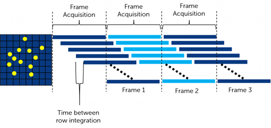
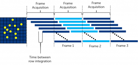
Schematic indicating how the acquisition of a frame can overlap with the readout of the previous frame. This allows the sCMOS to acquire and readout at a fast speed. Source: https://www.princetoninstruments.com/learn/camera-fundamentals/scmos-the-basics
The choice among a CMOS or sCMOS sensor relies on various factors. When comparing the two, you probably use the epifluorescence illumination since the white light is vivid enough to not depend on an sCMOS sensor.
The choice between the two simplifies when considering the amount of light approaching the camera or a blend of performance parameters exceptional to a particular application. Irrespective of sCMOS or CMOS, you must prioritize a monochrome sensor over the color equivalent sensor. This is because a monochrome sensor offers high quantum efficiency.
Two essential characteristics of sCMOS sensor include backside illumination and big pixels that help decrease the overall noise. Furthermore, sCMOS cameras typically incorporate a Peltier cooling mechanism to reduce thermal noise over extended exposures.
Those cameras equipped with sCMOS sensors also require a high bandwidth interface like CoaXpress or CameraLink with a frame grabber board, making these vision systems more complicated and, therefore, more expensive.
To counteract this, CMOS manufacturers have brought noteworthy enhancements in quantum efficiency, decreasing read noise and employing backside illumination.
The high quantum efficiency improves the incoming photon gathering ability. The reduced read noise guarantees that even the low levels of incoming photos are not lost in this noise.
Peltier cooling is also an alternative in a few CMOS sensors. But the boost in quantum efficiency and decreased noise has made cooling needless for several biomedical imaging applications.
CMOS sensors have been combined with interfaces like GigE, 10 GigE, and USB3. This is one of the ways to keep costs down. Such interfaces don’t need a frame grabber that decreases the cost and complexity of the system. Forthcoming interfaces like CXPX, USB4, and 25/100GigE will help to solve this problem by offering considerably higher bandwidths.
CMOS Sensors are an Affordable Alternative:
The affordable cost is one of the key factors encouraging many system designers and engineers to consider assessing the cutting-edge CMOS sensors over an sCMOS-based system.
In many instances, vision system designers are stunned to get a relevant CMOS camera for a price below $1,000 when a classic sCMOS setup with similar performance metrics could cost up to $10,000.
Irrespective of CMOS or sCMOS type, several camera manufacturers don’t use a single standard when comparing cameras. Therefore, it cannot be easy to compare cameras irrespective of the sensor type.
In the machine vision domain, EMVA1288 is the accepted standard for specifications and measurement of the cameras in America (AIA – American Automated Imaging Association), Japan (JIIA – Japan Industrial Imaging Association), and Europe.
Summing up, sCMOS cameras may be a requisite for cases requiring high-performance levels. However, it would be worthwhile to recognize the crucial performance metrics for a particular application. Moreover, it is essential to establish an unbiased comparison between CMOS and sCMOS cameras before making a choice.
There is continuous advancement in CMOS sensors. Moreover, the price-to-performance ratio between these two camera types is quickly narrowing. If a conventional CMOS sensor can meet your application requirements, it may be a cost-effective alternative.
When you are opting to shoot your images using a DSLR or phone camera, one of the most critical aspects that you need to focus on is choosing the correct image format. Most cameras or even smartphones make use of either JPG and RAW formats. What if you are a newbie and want to check the differences between the RAW and JPG images? We will also check out the features of NEF files.
What is a JPG file?
As you might have understood, a JPG or JPEG file – pronounced as jay-peg is an image file. In contrast, a few JPG files come with .jpg or .jpeg extensions. However, the difference lies only in the wing; they are the same file formats and do not have any difference.
The JPG files are used quite widely due to the compression algorithm that the file uses. This can be effective in helping you in reducing the size of the file. This can make it a great choice to work with a wide range of application areas, such as sharing, storing, and displaying them on blogs and websites. It may, however, be noticed that the compression also considerably reduces the image’s quality. If the image is compressed to a vast extent, it can be visible in many cases.
The JPG image format is one of the most common formats used in digital cameras. You would find supporting apps on multiple operating systems and on the internet. The JPG images generally employ a compression ratio of 10:1. Which will ensure that you will not lose any significant details. The degree of compression in the JPG files is much adjustable. The JPG images can be an excellent choice for photographs and realistic illustrations. They can also be a great option for the basic editing pursuits.
JPG files are also known to be a universal image format. The image format is identified and recognized by almost all internet browsers. It is the raster image format, and you would find it not the right one to use with the text.
The JPG files are pretty flexible. The invasive compression is what would make it a little disturbing. It is a great choice to help you with the best printing solution.
What is a RAW file?
RAW files are yet another image format captured on digital cameras. These image formats are known to provide lossless image quality, ideal for post-processing. The image format is used for capturing the image with all the details captured by your camera. The format saves your pictures in an unprocessed and uncompressed format.
Any image with the image sensor can shoot a picture in RAW. It can either be through the camera sensor or a host of image scanners. The RAW format takes the details from the sensor and produces a file with no processing whatsoever. The RAW files offer you a 14-bit color channel. That would mean the info on the image is sorted in much greater detail.
Unlike the JPG files, which most programs and software tools can open, you would be able to open them only with a few specialized software tools. When an image is shot on a digital camera, it is in the form of raw data. If the default format is set to JPEG, the raw data is processed, and the file is saved as a JPG or JPEG image.
If you set the image format to RAW, no processing is applied, so the file is saved with more tonal and color data. The RAW form is the one that is digitally tied and decided by a camera model.
A RAW image file typically consists of three essential components – the actual RAW data from the image sensor, a camera-processed full-size JPEG preview + thumbnail, and all relevant header and metadata information. One of the primary advantages you stand to gain with the RAW images as opposed to the JPG images is that the RAW file comes with a more comprehensive dynamic range and color gamut options.
What is a NEF file?
A NEF file is a RAW file created by Nikon cameras. In essence, a NEF file is a Nikon RAW file. It refers to the Nikon Electronic Format. This file format is solely used for and by the Nikon cameras. If you want to use software to open a NEF file, you can do it only with a tool compatible with the Nikon cameras.
Like a RAW file, the NEF file also captures all the data associated with your image. It takes into account all the data that your camera captures. It retains all the information in the picture captured by the camera. The details include the metadata in the camera and the lens model.
NEF is a lossless format, and you would find it one of the excellent options that you would find quite impressive. It can be a perfect option to help you get the best results from your Nikon camera. The NEF files are based on the TIFF format. They support 12-bit or 14-bit data, largely depending on the camera model that took the image. The NEF files store all the data related to the image and the camera it was shot on. This would include the details such as the settings like white balance, hue, tone, and sharpening.
How do RAW, JPG, and NEF file formats differ?
In a way, both RAW and NEF file formats belong to the same category. The only difference being the RAW format is a generalized format, and NEF is a specific RAW format used by the Nikon cameras. So, we will undertake the differences and details of a RAW vs. JPG format in finer detail.
RAW Format
The Advantages
It offers you more shadows of color
You can get a more comprehensive dynamic range and color gamut
An option for more refined control and adjustment options
You can adjust color space even after the image capture
It can be used to convert to other RAW formats
It provides you with a better degree of performance in ownership and authenticity.
The Disadvantages
It needs to go through the post-processing
It would require more storage
Issues with sharing
It can also need more file management options
Backups will take longer
JPG Format
The Advantages
It is also already processed, so it does not need further processing
A smaller size
No issues with the camera slowing down
It offers you multiple choices for compression
Faster backup capability
The Disadvantages
A lossy compression
It is just an 8-bit format
Recovery options are pretty limited
Camera settings can impact the image quality
Should you go with JPG or RAW image format?
The advantages of shooting RAW images can be a great option over using JPG. Since storage has gone relatively cheap these days, the storage issues that we once faced with the RAW images should not be a concern now.
In case you have been shooting a massive list of images and tend to get a poorly exposed photo, JPG can be the wrong choice. With a JPG, you will not have much to edit the idea to make it usable. On the contrary, shooting a photo in RAW will help you edit it much to your needs if you have rare and memorable moments to shoot. Doing so with the RAW format would be a great option. That way, you would always have an opportunity to improve your image even when it was shot with lousy exposure or other issues.
In Conclusion
That was a complete review of the differences between the NEF, JPG, and RAW images. Of course, each has its advantages, and it is always a good idea to check for the best benefits each image format offers. We would find each of them offering you one of excellent option in the long run.
If you are comparing sCMOS vs qCMOS sensors to understand their differences better, we have an article for you.
Two of the latest CMOS sensors prevalent today are sCMOS and qCMOS sensors. They significantly contribute to the advancement of CMOS technology.
sCMOS stands for Scientific complementary metal-oxide-semiconductor. It is a type of CMOS image sensor (CIS) with strict noise specifications. It entered its 4th generation era last year. These sensors are commonly used in applications associated with astronomy or biomedical imaging. But owing to its outstanding resolution capability, it is also now implemented in alternative vision applications.
BAE Systems’ latest sCMOS Hawkeye claims to be the foremost CMOS image sensor (CIS) to capture imagery in dull nighttime conditions. The HWK1411 is designed for unmanned platforms, battery-operated soldier systems, and targeting and surveillance applications.
During the start of 2021, Hamamatsu released details on a next-gen CIS known as quantitative CMOS (qCMOS). Developed on the ORCA-Quest camera system, qCMOS is believed to be competent in determining photon count using the industry-leading readout noise of 0.27 electrons RMS.
Suppose you want to understand why sCMOS and qCMOS technologies are significant to the military or scientific community. In that case, you should be familiar with an overview of the image sensor technology that evolved during the last couple of decades.
For more than ten years, charge-coupled device (CCD) technology was the top choice for advanced scientific imaging technology. But, since 2009, the development in scientific CMOS image sensor technology has principally pushed CCD devices unpopular. Generally, sCMOS technology provides higher speed frame rates, lower noise, and a giant field of view.
Image Sensor type
Largest use period
Pixels
Frame rate (fps)
Readout noise (electrons RMS)
Multiplication noise
Peak QE (%)
CCD
The 1990s to 2000s
1344 x 1024
16.2
6
No
70
EM-CCD
From the 2000s to 2010s
512 x 512
32
<1
Yes
97
Gen II sCMOS
2011to 2020
2048 x 2048
100
1.4
No
82
Gen III sCMOS
2018 till today
2304 x 2304
89.1
0.7
No
95
The advancement of the CMOS image sensors began to accelerate during the 1990s. However, the first generations of CMOS technology didn’t compete with CCD on quantum efficiency (QE).
It was the year 2011 when a newer generation of sCMOS enhanced QE up to 72% – 82% and decreased the read noise to the level where sCMOS will surpass CCD in several applications. The latest technology, known as the Gen III sCMOS, has entirely overlooked the potential of CCD/EM-CCD image sensors.
In 2021, the general CMOS sensor image technology depicted better quantum efficiency and reduced read noise. Therefore, the technology above may be an appropriate alternative to sCMOS. The cost factor among the two image sensors can be 10x, so this aspect makes CMOS a clear winner from a cost perspective, especially in the most demanding biomedical image applications.
To have a clear understanding, let’s get the basic details of sCMOS and qCMOS sensors:
What is sCMOS sensor?
sCMOS is technology dependent on the next-generation CMOS Image Sensor (CIS) design and fabrication techniques. The sCMOS image sensors provide fast frame rates, low noise, broad dynamic range, high resolution, high quantum efficiency, and a giant field of view concurrently in one image.
In the preliminary phases of CMOS development, the sCMOS technology was invented to eliminate the gap between the latest CMOS sensors and traditional CCD (Charge Coupling Device) sensors.
Initially, biomedical applications were inefficient in using CMOS sensors owing to the compromises in dynamic range, read noise, resolutions, and frame rates.
But when sCMOS cameras were initially invented, they used identical design principles and fabrication techniques to CMOS sensors. Also, it included various features that assisted them in tackling the preliminary shortcomings of CMOS. Consequently, sCMOS sensors are perfect for those scientific applications where low light performance, broad dynamic range, and high fidelity are inevitable.
Image acquisition starts at the top of the sensor and reaches down, row by row. Consequently, the sensor can capture images at higher framerates with lower read noise. Note that the speed of an sCMOS camera is directly related to the number of rows and the row time (the time between capturing one row and another).
What is a qCMOS sensor?
The qCMOS sensor will attain outstanding readout noise performance through cutting-edge CMOS technologies. The detection limit under ultra-low light conditions can be enhanced using a qCMOS sensor. qCMOS image sensor technology employs three measures to guarantee maximum sensitivity. These measures are BSI (back-side illumination), DTI (profound trench illumination), and Microlens. To restrict the effects of spatial crosstalk, the qCMOS sensor camera uses a DTI structure.
The number of pixels in traditional scientific cameras is, for instance, 4.2 MP with 6.5 μm pixel size or 1 MP with 13 μm pixel size. But with 9.4 MP, the qCMOS camera offers more than double the pixel count of a high-performance Gen II sCMOS camera.
The qCMOS camera realizes the particular photon number resolving apart from the temporal photon number resolving. Moreover, these cameras are also equipped with a special mode known as ‘photon number resolving mode.’ It can output the digital data as a photon number by calculating the digital output data from the AD converter to the photon number through real-time photography.
Note that the qCMOS sensor camera is the first cutting-edge camera implemented with photon number resolving capability.
Now let’s go through Bae Systems’ latest sCMOS.
Bae Systems’ Hawkeye Enables Superior Night Vision:
The Hawkeye sCMOS features a resolution of 1.6 MP (1440 x 1104) and operates at a maximum frame rate of 120 fps. This system has an ADC resolution of 11 bits and a programmable gain of 8x, 16x, and 32x.
The pixel size is 8.0 µm x 8.0 µm. The big pixel size reduces noise, an essential requirement for sCMOS technology.
The interface includes a 4-lane MIPI CSI-2 output interface, working at 1.5 Gbps/lane, with a control interface of SPI 40 MHz. Moreover, Hawkeye consumes power of less than 750 mW @ 120 fps with the operating temperature range from -40 ℃ to +85 ℃.
To improve CMOS technology, Hamamatsu achieves a milestone with its qCMOS sensor.
Hamamatsu’s qCMOS Claims 0.27e- Read Noise:
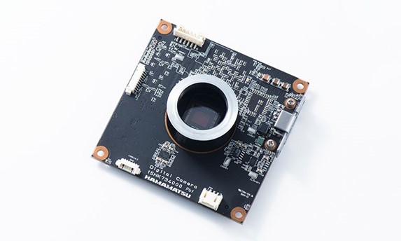
Notwithstanding the developments of sCMOS 3.0 in 2018, which featured a readout noise of 0.7 electrons RMS, still more work needs to be done. Hamamatsu has released the ORCA-Quest, the primary scientific camera in its line-up to implement the latest qCMOS image sensor technology.
The ORCA-Quest features a readout noise of 0.43 electrons RMS (Typ.) along with an ultra-quiet scan of 0.27 electrons RMS. When it comes to the quantization of discrete photoelectrons, the readout noise is a critical parameter.
Hamamatsu invented the term “qCMOS” to express the potential of “photon number resolving.” It implies measuring light by calculating photoelectrons.
As seen from the below graph, the ability to detect individual photoelectrons vanished for a readout noise of 0.5 electrons and higher.
Hamamatsu keeps driving innovation and development for the CMOS technology by introducing the qCMOS architecture. In the meantime, Bae Systems is working on adopting sCMOS technology in many fields apart from scientific imaging.
Afar sCMOS, the industry has perceived advancements in image sensor technology for various applications in 2021.
In this post, we are comparing Samsung’s ISOCELL Plus vs EXMOR-RS CMOS sensor by Sony semiconductor. Both imaging sensors are built for entirely different camera form factors. The Sony sensors are for their flagship range of mirrorless cameras, whereas ISOCELL+ is for smartphones.
ISOCELL Plus and EXMOR-RS CMOS sensors improve image quality in the latest camera models. Let’s go through the details of each of them:
ISOCELL Plus sensor:
The latest ISOCELL Plus sensor technology from Samsung powers the top-notch cameras seen on the brand’s flagship devices. Samsung tackled the engineering challenges of smartphone cameras and built the ISOCELL Plus technology, which pushes the boundaries of the image sensor to convey color-accurate, crystal-clear photos even in challenging lighting conditions.
ISOCELL technology enables a broader chief ray angle (CRA) by capturing more diagonal light. This eventually allows a brighter lens with a wider aperture that produces clear and more luminous pictures even in low light conditions.
Because of their design, ISOCELL image sensors can also decrease the height of the camera module irrespective of the resolution. Hence, these sensors adopt the sleek form factor of contemporary smartphones.
Five years after the inception of ISOCELL, Samsung has elevated the image sensing technology further with the ISOCELL Plus.
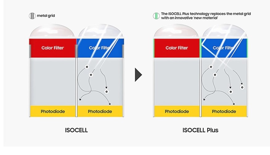
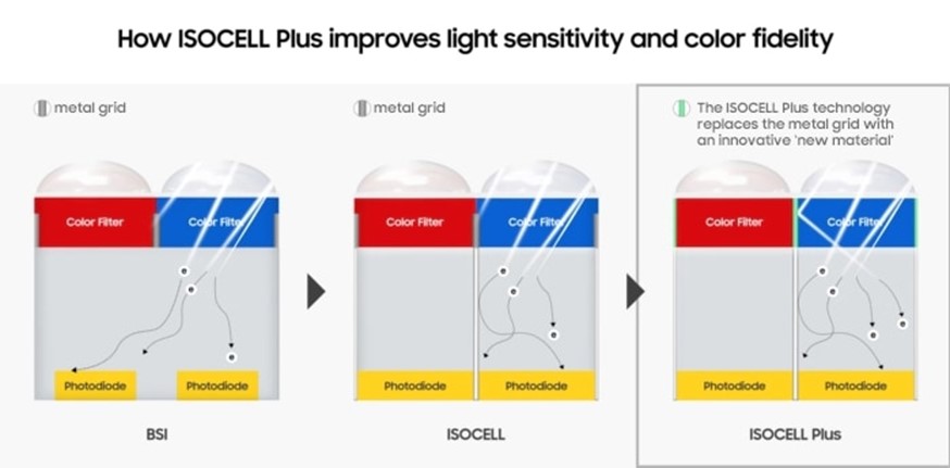
In the traditional ISOCELL technology, the metal grids that isolate the color filter decreases interference between pixels. Also, they lead to some optical loss because they absorb reflected light or incoming light from the neighboring pixels.
On the other hand, the ISOCELL Plus sensor substitutes that metal barrier with an advanced new material developed by Fujifilm. So, it minimizes light reflection and optical loss. The latest ISOCELL Plus technology indicates more accurate and sharper photos, although challenging light environments exist.
The ISOCELL Plus sensor features higher color fidelity and 15% more light sensitivity. Moreover, this sensor is compatible with super-resolution cameras with more than 20 MP resolutions. The technology also allows the image sensor to equip pixel-sized 0.8 µm or smaller without any performance loss. Hence, this sensor is an optimal solution for high-resolution cameras.
ISOCELL Plus sensor not only facilitates the development of ultra-high-resolution sensors with its small pixels but will also provide a performance boost for sensors with more significant pixel designs. The pixels are separated through a unique coating material, leading to a rise in density by 30%.
Samsung launched ISOCELL Plus in July 2018, and since then, it has progressively extended its image sensor lineup built on the technology.
Exmor-RS CMOS sensor:
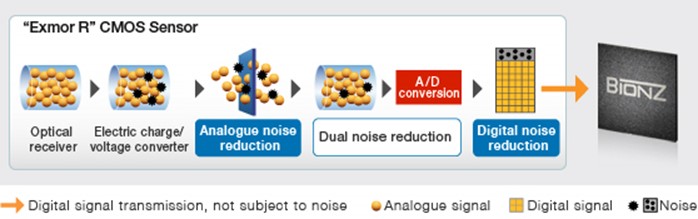
Sony developed Exmor-RS, the world’s foremost stacked CMOS image sensor that conveys superior picture quality in a compact size. It is designed for use in tablets and smartphones. It includes a unique, advanced ‘stacked structure.’
Sony built this 35 mm full-frame stacked CMOS image sensor with the built-in memory for the high-performance α9. It leads to a lighter and smaller professional camera.
In addition to offering outstanding imaging performance, it entails multiple functions that help reduce components to trim the weight and size of the α9. The idea behind the development is to use natural resources. The structure layers the pixel section that shows results of back-illuminated pixels on the chip attached with mounted circuits for signal processing.
This α9 sensor significantly boosts image quality and performance through powerful AF; vibration-free, silent, constant shooting up to 20 fps, and a blackout-free viewfinder. Note that this sensor packs all the features of a conventional digital SLR mirror, AF sensor, mechanical shutter, and optical finder.
Along with these, it reduces the physical size and weight of the camera. Compared to a conventional full-frame DSLR, for example, Sony’s first full-frame model α900, the α9 is approx. 20% smaller. So, it is easier to carry anywhere. Moreover, this sensor offers performance and speeds beyond the capabilities of other sensor models while using fewer resources.
Sony will also unveil three corresponding imaging modules equipped with these sensors. Of these three modules, two Exmor-RS models that Sony will launch are IMX135 (type 1/3.06 model with 13.13 effective megapixels) and IMX1344 (type 1/4 model with 8.08 effective megapixels). They feature the ‘HDR (High Dynamic Range) movie’ function and the ‘RGBW coding’ function.
HDR movie function allows the configuration of two unique exposure conditions on a single screen when shooting. It flawlessly performs image processing to produce optimal images with brilliant colors and a broad dynamic range, irrespective of the light conditions.
RGBW coding function can capture clear, sharp images even when captured in low light conditions. This function features W (white) pixels in addition to the conventional RGB (red-green-blue) pixel. It leverages Sony’s proprietary device technology and signal processing to enhance sensitivity without negotiating its high resolution.
The third Exmor RS imaging module is the ISX014 (type 1/4 model with 8.08 effective megapixels). It has an in-built camera signal processing function.
Critical features of Exmor RS stacked CMOS image sensor:
Commercializing the latest, independently developed Exmor-RS, equipped with the world’s first unique stacked structure.
The corresponding stacked structure offers superior image quality and a more compact size.
Implemented with ‘HDR movie’ and ‘RGBW coding’ functions (“IMX135” and “IMX134”)
It is implemented with a built-in camera signal processing function that provides compatibility with picture adjustment, automatic controls, and multiple image output formats (like YUV) (“ISX014”).
ISOCELL Plus vs. EXMOR-RS CMOS sensor:
ISOCELL Plus sensor
Exmor-RS CMOS sensor
Compatible with cameras with a resolution of more than 20 MP
Compatible with cameras with resolution up to 13.3 MP
Equip pixels of size 0.8 µm or smaller without any performance loss
The corresponding camera models are 20% smaller than full-frame DSLR cameras
Improves the image quality using higher color fidelity and 15% more light sensitivity
Improves the image quality and performance using powerful AF; constant shooting up to 20 fps, and a blackout-free viewfinder
The output minimizes optical loss and light reflection
The optimal image output shows brilliant colors, sharpness, clarity, and a broad dynamic range, irrespective of the light conditions
When a network camera captures an image, the light passes across the lens and impinges on the image sensor. In addition, the image sensor also contains picture elements known as pixels which record the amount of light that falls on them.
These pixels transform the received light into a relevant number of electrons. The intensity of the light is proportional to the number of electrons generated. These electrons are converted into voltage and subsequently transformed into numbers through an A/D-converter. Consequently, the signal created by the numbers is processed through electronic circuits within the camera.
Overview of image sensors:
The original argument a decade ago for the renewal of CMOS image sensors as a competitor to CCD technology was generally based on several ideas:
1- Lithography and operation control in CMOS fabrication had reached tiers that soon would allow CMOS sensor image quality to rival CCDs.
2 – Integration of companion functions on the same die as the image sensor, creating camera-on-a-chip or SoC (system-on-a-chip) capabilities.
3 – Reduced power consumption.
4 – Decreased imaging system size because of integration and reduced power consumption.
5 – Using the identical CMOS production lines as mainstream logic and memory device fabrication, delivering economies of scale for CMOS imager manufacturing.
Currently, two key technologies are prevalent for the image sensor in a camera. They are CMOS (Complementary Metal-oxide Semiconductor) and CCD (Charge-coupled Device). The following sections explain their design and varied strengths and weaknesses.
Initial Prediction for CMOS
Twist
Outcome CMOS vs. CCD
Equivalence to CCD in image performance
Required much greater process adaptation and deeper submicron lithography than initially thought
High performance is available in both technologies today, but with higher development costs in most CMOS than CCD technologies.
On-chip circuit integration
Longer development cycles, increased cost, trade-offs with noise, flexibility during operation
Greater integration in CMOS than CCD, but companion ICs still often required with both
Economies of scale from using mainstream logic and memory foundries
Extensive process development and optimization required
Legacy logic and memory production lines are commonly
used for CMOS imager
production today, but with highly adapted processes
akin to CCD fabrication
Reduced power consumption
Steady progress for CCDs diminished the margin of improvement for CMOS
CMOS ahead of CCDs
Reduced imaging subsystem size
Optics, companion chips, and packaging are often the dominant factors in imaging subsystem size.
Comparable
Color filtering:
Image sensors record the amount of light from the bright to the dark region with no color information. Because CCD and CMOS image sensors are ‘color blind,’ a filter at the front of the sensor enables the sensor to allocate color tones to every pixel.
In this context, two widespread color registration techniques are CMYG (Cyan, Magenta, Yellow, and Green) and RGB (Red, Green, and Blue). Red, green, and blue are the primary colors, which, when combined in varied combinations, can generate the majority of the colors visible to the human eye.
The Bayer array represents the alternating rows of green-blue and red-green filters. It is the ubiquitous RGB color filter. Because the human eye is more sensitive to green color compared to the other two colors, the Bayer array features twice as many green color filters. It implies that when using the Bayer array, the human eye can sense more detail than when all the three colors were used in identical measures in the filter.
An alternate method to filter or record color is to use complementary colors, i.e., cyan, magenta, and yellow. Frequently, the complementary color filters on sensors are merged with green filters to create a CMYG color array. Generally, the CMYG system provides higher pixel signals owing to its broader spectral bandpass.
But, the signals should be subsequently transformed into RGB because this is used in the final image. The conversion indicates added noise and more processing. The outcome is that the initial gain in the signal-to-noise is decreased. Note that the CMYG system is not so efficient at accurately presenting colors.
Usually, the CMYG color array is used in interlaced CCD image sensors. On the other hand, the RGB system is prominently used in progressive scan image sensors.
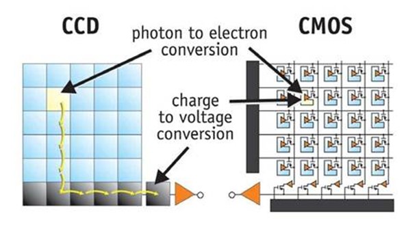
In a CCD sensor, the light impinges on the sensor’s pixels and is conveyed from the chip via one output node or merely a few output nodes. These charges are then transformed into voltage levels, buffered, and delivered as an analog signal. The particular signal is finally amplified and converted to numbers through an A/D-converter exterior to the sensor.
Specifically, the CCD technology was developed to be used in cameras. For over 30 years, the CCD sensors have been utilized. Conventionally, these sensors offered some benefits compared to the CMOS sensors, including less noise and improved light sensitivity. However, these differences have vanished in recent years.
The limitations of CCD sensors are that analog components need more electronic circuitry exterior to the sensor. Also, their production is costly and can consume up to 100 times more power than CMOS sensors. Due to the increased power consumption, there can be heat concerns in the camera. This not only influences image quality negatively but also raises the cost and environmental effect of the product.
Also, CCD sensors need a higher data rate because everything has to pass through only one output amplifier or some output amplifiers.
CMOS technology:
In the beginning, ordinary CMOS chips were deployed for imaging purposes. But the output showed poor image quality because of their inferior light sensitivity. The contemporary CMOS sensors implement a more dedicated technology. Moreover, the light sensitivity and quality of the sensors have quickly augmented in recent years.
CMOS chips provide various advantages. Contrasting the CCD sensor, the CMOS chip includes A/D-converters and amplifiers, reducing the camera expense because it comprises all the logic required to generate an image. All CMOS pixel comprises conversion electronics.
Compared to CCD sensors, CMOS sensors feature better integration possibilities and more functionality. But, this inclusion of circuitry within the chip poses a risk of more structured noise like stripes and other patterns. Moreover, CMOS sensors come with higher noise immunity, lower power consumption, a faster readout, and a smaller system size.
Calibrating a CMOS sensor in production (if needed) can be more challenging than calibrating a CCD sensor. However, technological advancement has made CMOS sensors easier to calibrate. Some of them are currently self-calibrating too.
It is allowed to read individual pixels from a CMOS sensor. This enables ‘windowing,’ which suggests that it is possible to read out the parts of the sensor area rather than the whole sensor area at once.
Consequently, a higher frame rate can be conveyed from a restricted part of the sensor; digital PTZ (pan/tilt/zoom) functionalities can also be used. With a CMOS sensor, it is also possible to obtain multi-view streaming that enables various cropped view areas to be simultaneously streamed from the sensor, ultimately simulating some ‘virtual cameras.’
HDTV and megapixel sensors:
HDTV and Megapixel technology allows network cameras to deliver higher resolution video images compared to analog CCTV cameras. This aspect implies that they expand the possibility of observing details and recognizing objects and people. This is a major consideration in video surveillance applications.
An HDTV or megapixel network camera provides a minimum of twice as high a resolution as a conventional, analog CCTV camera. Megapixel sensors are fundamental components in HDTV, megapixel, and multi-megapixel cameras. They can be used to present very detailed images as well as multi-view streaming.
Megapixel CMOS sensors are extensively available and usually less expensive compared to megapixel CCD sensors. However, there are myriad examples of costly CMOS sensors.
It is tough to create a fast-megapixel CCD sensor. It is a disadvantage and increases the complexity of developing a multi-megapixel camera through CCD technology.
Many megapixel camera sensors are usually identical in size to the VGA sensors, with a resolution of 640×480 pixels. A megapixel sensor includes more pixels than a VGA sensor. Therefore, the size of every pixel in a megapixel sensor converts smaller than that in a VGA sensor.
Consequently, a megapixel sensor is usually less light sensitive per pixel than a VGA sensor. The reason is the pixel size is smaller, and the light reflected from an object spreads to more pixels. But, this technology is swiftly enhancing megapixel sensors. Furthermore, the performance in context to light sensitivity is continuously improving.
Key differences:
A CMOS sensor includes A/D-converters, amplifiers, and circuitry for extra processing. On the other hand, in a camera equipped with a CCD sensor, several signal processing functions are carried out exterior to the sensor.
A CMOS sensor permits multi-view streaming and windowing, which can’t be accomplished with a CCD sensor. Generally, a CCD sensor has one charge-to-voltage converter in each sensor. On the other hand, a CMOS sensor has one charge-to-voltage converter in each pixel. Due to the faster readout, a CMOS sensor is more suitable for use in multi-megapixel cameras.
The latest technology advancements have eliminated the difference in light sensitivity between a CMOS and CCD sensor at a specified price point.
Detailed Comparison of CCD and CMOS sensors:
i. System Integration:
Being an old technology with a CCD sensor, it is impossible to integrate peripheral components like ADC and timers into the primary sensor. Hence, additional circuitry is required, increasing the CCD sensors’ overall size. Furthermore, specialized fabrication techniques are used in making CCD sensors, so it is expensive technology.
The camera can be incorporated into the chip or system in CMOS sensors. Hence, the CMOS sensors are very compact.
ii. Power Consumption:
CCD sensors feature higher power consumption compared to CMOS sensors due to the capacitive architecture. Various types of power supplies are required for the varied timing clocks. The typical voltage for the CCD sensors falls in the range of 7 V to 10 V.
CMOS sensors offer low power consumption compared to CCD sensors because it needs a single power supply. The range of typical voltage is usually 3.3 V to 5 V. So, for the application wherein power consumption is the key criterion, the CMOS sensor is preferable to the CCD sensor.
Since CMOS sensors feature a lower power consumption compared to CCD image sensors, the temperature within the camera can be maintained lower. Moreover, heat issues with CCD sensors can enhance interference. On the other hand, CMOS sensors can have higher structured noise.
iii. Processing Speed:
CCD sensor always needs to read out the entire image, resulting in less processing speed. It is possible to increase it using the multiple shift registers. However, this will demand additional hardware.
In the CMOS sensor, the readout for the particular area of an image is possible; therefore, its speed is higher than the CCD sensor. This speed can be further increased by utilizing the multiple column select lines. Note that the dynamic range of the CCD sensor is considerably higher than the CMOS sensor.
iv. Image distortion:
A blooming effect is visible when a CCD sensor is exposed for an extended period. With the anti-blooming technique, this blooming effect can be reduced.
In a CCD sensor, all the pixels are exposed at once. Hence, if you intend to eliminate the rolling shutter effect, all the pixels must be exposed at the same time. This is called the global shutter effect. So, these days, the CMOS sensors are equipped with global sensors. Since the entire frame is captured at once, there are no wobble, skew, smear, or partial exposure effects.
The most common kind of distortion in CMOS sensors is the rolling shutter. This is because, in the CMOS sensor, the pixels are read line by line. Hence, whenever any quickly moving object gets captured by this CMOS sensor, the rolling shutter effect becomes significantly noticeable.
All portions of a frame are not captured at a time but separately. Subsequently, all parts are showcased at once. As a result, it may add a time lag in frames. So, the images may wobble or undergo a skew effect. But, the high-end CMOS cameras contain more efficient sensors.
v. Noise and Sensitivity:
CMOS sensors have more noise owing to the higher dark currents. The reason is the charge to voltage converter circuit and amplification circuit is incorporated into the same pixel. Hence, the overall fill factor of the CMOS sensor is lesser than the CCD sensor. Consequently, the sensitivity of the CMOS sensor will be lesser than that of the CCD sensor.
In the CMOS sensor, the amplifiers used in every pixel are different. Due to that, we will notice the non-uniform amplification, which would behave as additional noise. However, the technology of this CMOS sensor has progressed so much that the sensitivity and noise of this CMOS sensor are identical to the CCD sensor.
vi. Construction:
CCD chips register the pixels (whenever light strikes) on the chip and subsequently send these pixels one by one. Hence, the time required for transmitting the pixels for one image increases. Because of continuous fetching and sending activities, the chip consumes a lot of power.
In CMOS sensor chips, the sensors themselves have plenty of inbuilt circuitry. This allows reading the pixels at the photo sensor level itself. The detailed data is sent all at once. Hence, there is no time lag, and less energy will be consumed due to this activity.
vii. Vertical Streaking:
When the CCD sensor-based cameras are used in video or live mode, they demonstrate vertical streaking. In these images, a bright vertical line is formed. Because plenty of analog sensors exist in a row, the current that overflows one of the sensors will leak to the entire row. Hence, it creates a vertical line. But, in other modes, CCD sensors don’t exhibit such characteristics.
There are no such concerns in CMOS sensors because every circuit is completely isolated from the remaining circuits on the chip.
viii. Image quality:
CCD sensors boast lower noise levels since their layout enables more pixels to be recorded over their surface. Therefore, the colors of the captured images are more vibrant. As a result, it enhances the image quality.
Conversely, due to their layout, CMOS sensors can’t accommodate more pixels over their surface. Hence, images will have low resolution, which negatively influences image quality.
Because the CCD technology is more advanced than the CMOS technology, the image quality is better. But the drawback of the technology is its higher power consumption and streaking issues.
ix. Application:
CCD sensors are widely used in DSLR cameras. Conversely, due to lower cost and longer battery life, CMOS sensors are extensively used in mobile phones, tablets, digital cameras, etc.
CCD vs CMOS Sensor:
Parameters
CCD Sensor
CMOS Sensor
Resolution
Up to 100+ MP
Sensor elements’ size restricts resolution
More than 100 MP supported
Frame rate
Best for lower frame rates
Best for higher frame rates
Color depth
Higher (16+ bits is standard for expensive CCDs)
Lower (12-16 bits is standard)
Responsivity and linearity
Lower responsivity, wider linear range
Higher responsivity, lower linear range (will saturate early)
Limit of detection
Low (more sensitive at low intensity)
High (less sensitive at low intensity)
Noise figure
Lower noise floor leads to higher image quality
Higher noise floor leads to lower image quality
Conclusion:
CCD and CMOS sensors feature unique benefits. Both these technologies are rapidly evolving. The best suitable strategy for a camera manufacturer is to assess and test sensors for every camera being developed constantly. Subsequently, whether a selected sensor is based on CMOS or CCD becomes irrelevant. So, the only focus is the sensor that can be utilized to build a network camera that conveys the expected image quality and meets the customers’ video surveillance needs.
You can use a CCD sensor to benefit from better image quality and lower cost. You can use a CMOS sensor to help from faster readout speed, low power consumption, lower noise, longer battery life, and no time lag.
The latest ISOCELL Plus camera sensors from Samsung are all set to convey enhanced color accuracy, light sensitivity, and added light gathering capacity in smartphone camera technology. These improvements result from replacing the metal barriers among pixels with walls prepared from a new material.
Smartphone consumers can expect even more precise and clearer photos in dim light environments. CMOS image sensors will be implemented with the optimized pixel isolation technology to fetch these improvements.
In this context, Samsung states that the latest technology will lead to enhanced super-resolution mobile cameras. Although Samsung’s ISOCELL technology is a standard installation in smartphone sensors, it has announced the launch of its latest ISOCELL Plus technology. This technology guarantees enhanced color accuracy and light sensitivity from forthcoming smartphone cameras.
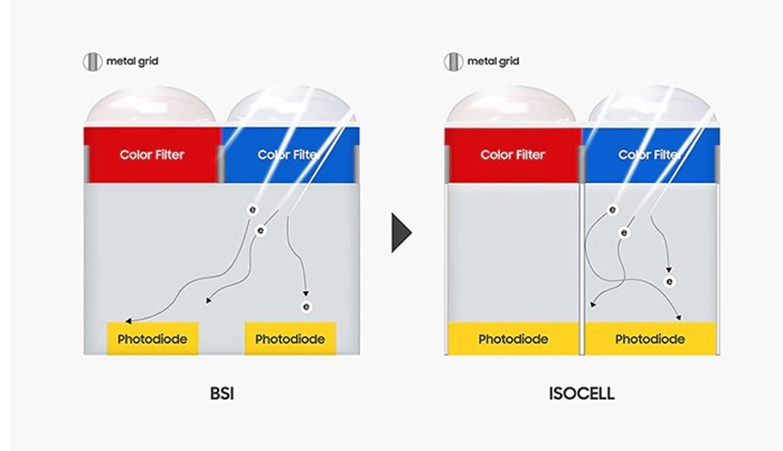
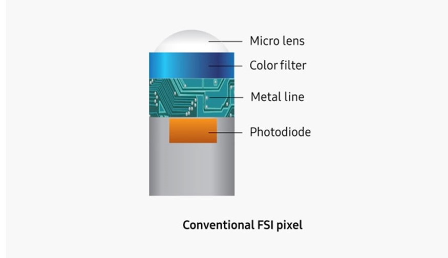
In the existing ISOCELL camera sensors, there is a physical metal barrier between pixels. The purpose of including this barrier is to decrease color cross-talk. However, the metal barrier poses a side-effect of reflecting or absorbing incoming light, which leads to reduced photo quality.
In the prevailing pixel structure, metal grids are created over the photodiodes to decrease interference between the pixels. This can also cause some optical loss as metals reflect and/or absorb the entering light. With the launch of the ISOCELL Plus, Samsung elevates the pixel isolation technology to a new level via optimized pixel architecture.
Image Source: Samsung
Essentially, the ISOCELL Plus technology substitutes that metal barrier with a fresh material developed by Fujifilm. This improves the photo quality by decreasing absorption/reflection and optical loss. Explicitly, Samsung claims a 15%improvement in light sensitivity and a boost in color fidelity.
To capture high-quality photographs, CMOS image sensors must hold maximum light as possible and then transmit the accurate color information to the photodiode. These requirements were solved by the launch of Samsung’s ISOCELL technology in 2013.
Image Source: Samsung
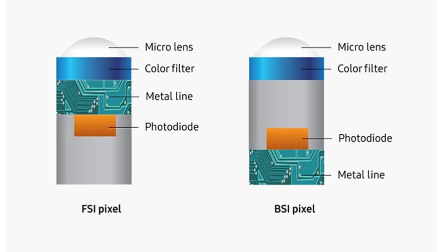
The formation of the physical barrier between adjacent pixels enables every pixel to absorb and retain more light than the traditional backside-illuminated (BSI) image sensor design for outstanding image quality.
The latest ISOCELL Plus Technology will benefit from higher resolution cameras:
Image Source: Samsung
ISOCELL Plus sensors will also be beneficial for higher resolution cameras. The company stated that the technology would permit 0.8 micron and smaller pixels. Therefore, it makes it perfect for super-resolution cameras with a resolution of more than 20 MP.
Most high-resolution smartphone cameras usually excel during the day but show poor performance at night. A large image sensor facilitates better night-time snaps (raising the phone’s thickness), pixel-binning (presenting brighter but lower-resolution snaps), or a dual-camera setup. But the Samsung’s latest ISOCELL Plus technology unlocks the door for another solution without compromising resolution or size.
This light-boosting technology can also benefit telephoto cameras, which usually depict poor performance in low light owing to their smaller apertures. Perhaps, it won’t present an extraordinary improvement in output quality at night. However, it can still be considered an improvement over existing telephoto zoom cameras.
In the context of this technology, Yanagihara, corporate vice president of Fujifilm, stated that they value their strategic relationship with Samsung. He added that this development is a noteworthy milestone for them because it records the first commercialization of their new material. He also stated that through constant cooperation with Samsung, Fujifilm expects to present more significant innovations to mobile cameras.
Ben K. Hur, the vice president of System LSI marketing at Samsung Electronics, said that with this collaboration with Fujifilm, an industry frontrunner in imaging and information technology, Samsung had elevated the boundaries of CMOS image sensor technology.
He added that the ISOCELL Plus technology would facilitate the development of ultra-high-resolution sensors with extraordinarily small pixel dimensions and convey performance advancements for the sensors with more significant pixel designs.
Samsung is exhibiting the tech at Mobile World Congress Shanghai (scheduled to conduct from June 27 to June 29). However, it hasn’t been declared when the first phones with ISOCELL Plus sensors will release. It is expected that we will soon have phones with this technology.










 sCMOS is technology dependent on the next-generation CMOS Image Sensor (CIS) design and fabrication techniques. The sCMOS image sensors provide fast frame rates, low noise, broad dynamic range, high resolution, high quantum efficiency, and a giant field of view concurrently in one image.
 Notwithstanding the developments of sCMOS 3.0 in 2018, which featured a readout noise of 0.7 electrons RMS, still more work needs to be done. Hamamatsu has released the ORCA-Quest, the primary scientific camera in its line-up to implement the latest qCMOS image sensor technology.
 The latest ISOCELL Plus sensor technology from
  Sony developed Exmor-RS, the world’s foremost stacked CMOS image sensor that conveys superior picture quality in a compact size. It is designed for use in tablets and smartphones. It includes a unique, advanced ‘stacked structure.’