

If you are comparing sCMOS vs qCMOS sensors to understand their differences better, we have an article for you.
Two of the latest CMOS sensors prevalent today are sCMOS and qCMOS sensors. They significantly contribute to the advancement of CMOS technology.
sCMOS stands for Scientific complementary metal-oxide-semiconductor. It is a type of CMOS image sensor (CIS) with strict noise specifications. It entered its 4th generation era last year. These sensors are commonly used in applications associated with astronomy or biomedical imaging. But owing to its outstanding resolution capability, it is also now implemented in alternative vision applications.
BAE Systems’ latest sCMOS Hawkeye claims to be the foremost CMOS image sensor (CIS) to capture imagery in dull nighttime conditions. The HWK1411 is designed for unmanned platforms, battery-operated soldier systems, and targeting and surveillance applications.
During the start of 2021, Hamamatsu released details on a next-gen CIS known as quantitative CMOS (qCMOS). Developed on the ORCA-Quest camera system, qCMOS is believed to be competent in determining photon count using the industry-leading readout noise of 0.27 electrons RMS.
Suppose you want to understand why sCMOS and qCMOS technologies are significant to the military or scientific community. In that case, you should be familiar with an overview of the image sensor technology that evolved during the last couple of decades.
Overview of History of Image Sensor Technology:
For more than ten years, charge-coupled device (CCD) technology was the top choice for advanced scientific imaging technology. But, since 2009, the development in scientific CMOS image sensor technology has principally pushed CCD devices unpopular. Generally, sCMOS technology provides higher speed frame rates, lower noise, and a giant field of view.
| Image Sensor type | Largest use period | Pixels | Frame rate (fps) | Readout noise (electrons RMS) | Multiplication noise | Peak QE (%) |
| CCD | The 1990s to 2000s | 1344 x 1024 | 16.2 | 6 | No | 70 |
| EM-CCD | From the 2000s to 2010s | 512 x 512 | 32 | <1 | Yes | 97 |
| Gen II sCMOS | 2011to 2020 | 2048 x 2048 | 100 | 1.4 | No | 82 |
| Gen III sCMOS | 2018 till today | 2304 x 2304 | 89.1 | 0.7 | No | 95 |
The advancement of the CMOS image sensors began to accelerate during the 1990s. However, the first generations of CMOS technology didn’t compete with CCD on quantum efficiency (QE).
It was the year 2011 when a newer generation of sCMOS enhanced QE up to 72% – 82% and decreased the read noise to the level where sCMOS will surpass CCD in several applications. The latest technology, known as the Gen III sCMOS, has entirely overlooked the potential of CCD/EM-CCD image sensors.
In 2021, the general CMOS sensor image technology depicted better quantum efficiency and reduced read noise. Therefore, the technology above may be an appropriate alternative to sCMOS. The cost factor among the two image sensors can be 10x, so this aspect makes CMOS a clear winner from a cost perspective, especially in the most demanding biomedical image applications.
To have a clear understanding, let’s get the basic details of sCMOS and qCMOS sensors:
What is sCMOS sensor?
 sCMOS is technology dependent on the next-generation CMOS Image Sensor (CIS) design and fabrication techniques. The sCMOS image sensors provide fast frame rates, low noise, broad dynamic range, high resolution, high quantum efficiency, and a giant field of view concurrently in one image.
In the preliminary phases of CMOS development, the sCMOS technology was invented to eliminate the gap between the latest CMOS sensors and traditional CCD (Charge Coupling Device) sensors.
Initially, biomedical applications were inefficient in using CMOS sensors owing to the compromises in dynamic range, read noise, resolutions, and frame rates.
But when sCMOS cameras were initially invented, they used identical design principles and fabrication techniques to CMOS sensors. Also, it included various features that assisted them in tackling the preliminary shortcomings of CMOS. Consequently, sCMOS sensors are perfect for those scientific applications where low light performance, broad dynamic range, and high fidelity are inevitable.
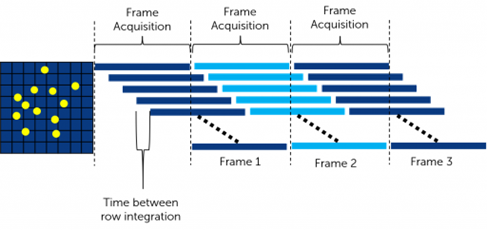
Image acquisition starts at the top of the sensor and reaches down, row by row. Consequently, the sensor can capture images at higher framerates with lower read noise. Note that the speed of an sCMOS camera is directly related to the number of rows and the row time (the time between capturing one row and another).
What is a qCMOS sensor?
The qCMOS sensor will attain outstanding readout noise performance through cutting-edge CMOS technologies. The detection limit under ultra-low light conditions can be enhanced using a qCMOS sensor. qCMOS image sensor technology employs three measures to guarantee maximum sensitivity. These measures are BSI (back-side illumination), DTI (profound trench illumination), and Microlens. To restrict the effects of spatial crosstalk, the qCMOS sensor camera uses a DTI structure.
The number of pixels in traditional scientific cameras is, for instance, 4.2 MP with 6.5 μm pixel size or 1 MP with 13 μm pixel size. But with 9.4 MP, the qCMOS camera offers more than double the pixel count of a high-performance Gen II sCMOS camera.
The qCMOS camera realizes the particular photon number resolving apart from the temporal photon number resolving. Moreover, these cameras are also equipped with a special mode known as ‘photon number resolving mode.’ It can output the digital data as a photon number by calculating the digital output data from the AD converter to the photon number through real-time photography.
Note that the qCMOS sensor camera is the first cutting-edge camera implemented with photon number resolving capability.
Now let’s go through Bae Systems’ latest sCMOS.
Bae Systems’ Hawkeye Enables Superior Night Vision:
The Hawkeye sCMOS features a resolution of 1.6 MP (1440 x 1104) and operates at a maximum frame rate of 120 fps. This system has an ADC resolution of 11 bits and a programmable gain of 8x, 16x, and 32x.
The pixel size is 8.0 µm x 8.0 µm. The big pixel size reduces noise, an essential requirement for sCMOS technology.
The interface includes a 4-lane MIPI CSI-2 output interface, working at 1.5 Gbps/lane, with a control interface of SPI 40 MHz. Moreover, Hawkeye consumes power of less than 750 mW @ 120 fps with the operating temperature range from -40 ℃ to +85 ℃.
To improve CMOS technology, Hamamatsu achieves a milestone with its qCMOS sensor.
Hamamatsu’s qCMOS Claims 0.27e- Read Noise:
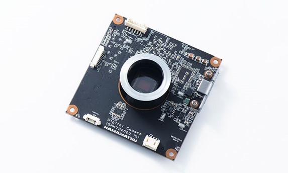 Notwithstanding the developments of sCMOS 3.0 in 2018, which featured a readout noise of 0.7 electrons RMS, still more work needs to be done. Hamamatsu has released the ORCA-Quest, the primary scientific camera in its line-up to implement the latest qCMOS image sensor technology.
The ORCA-Quest features a readout noise of 0.43 electrons RMS (Typ.) along with an ultra-quiet scan of 0.27 electrons RMS. When it comes to the quantization of discrete photoelectrons, the readout noise is a critical parameter.
Hamamatsu invented the term “qCMOS” to express the potential of “photon number resolving.” It implies measuring light by calculating photoelectrons.
As seen from the below graph, the ability to detect individual photoelectrons vanished for a readout noise of 0.5 electrons and higher.
Hamamatsu keeps driving innovation and development for the CMOS technology by introducing the qCMOS architecture. In the meantime, Bae Systems is working on adopting sCMOS technology in many fields apart from scientific imaging.
Afar sCMOS, the industry has perceived advancements in image sensor technology for various applications in 2021.