

Action cameras have evolved into specialized tools that serve very different purposes. Both the DJI Osmo Nano and the Insta360 Ace Pro 2 utilize a 1/1.3-inch sensor size, but their hardware design philosophies are polar opposites.
The Osmo Nano prioritizes extreme portability and flexible POV mounting for athletes and creators who need a “barely there” camera. Conversely, the Insta360 Ace Pro 2 functions as a full-sized flagship, packing 8K resolution, Leica optics, and extensive professional workflow features into a traditional rugged body.
Understanding these differences is key to picking the right gear for your next shoot. Below, we compare the design, imaging output, and real-world utility of both models.
LensXP
Updated till Feb 2026
DJI Osmo Nano vs Insta360 Ace Pro 2 Specs Comparison
Two very different approaches to action cameras using the same 1/1.3 inch sensor size.
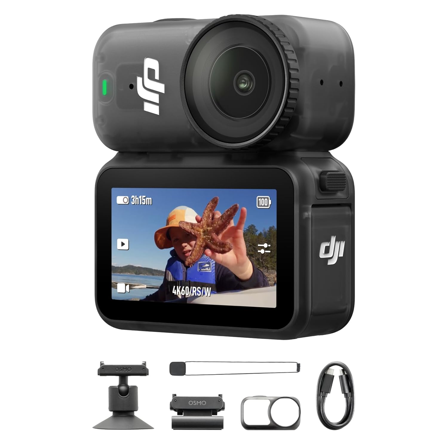
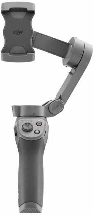
DJI Osmo Nano
An ultra compact wearable POV camera weighing just 52 grams for the camera module.
Check on Amazon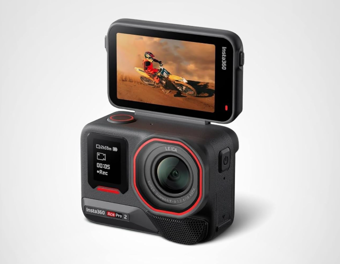
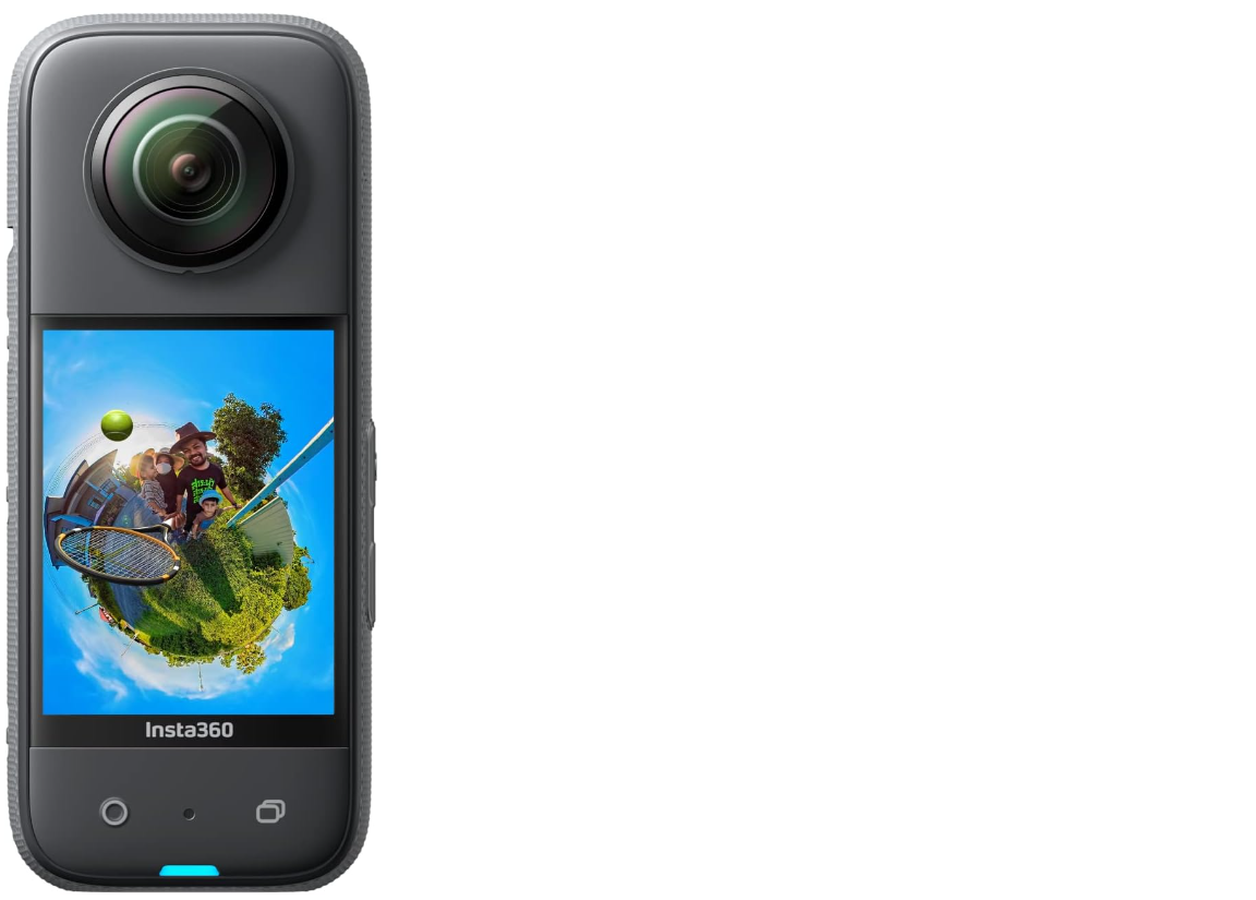
Insta360 Ace Pro 2
A full size action camera with an integrated flip up touchscreen weighing 184 grams.
Check on AmazonBoth cameras target very different use cases. The Osmo Nano relies on extreme portability and mounting flexibility. The Ace Pro 2 offers extensive creator features for serious video production. Below we compare their designs, key specifications, and ideal use cases.
Interactive Performance Chart
Core Specifications
| Feature | DJI Osmo Nano | Insta360 Ace Pro 2 |
|---|---|---|
| Sensor Size | 1/1.3 inch CMOS | 1/1.3 inch CMOS |
| Max Resolution | 4K at 60fps | 8K at 30fps |
| Lens & FOV | f/2.8 at 143 degrees | f/2.6 at 157 degrees |
| Waterproofing | 10 meters sealed module | 12 meters full unit |
| Battery | 530 mAh module plus 1300 mAh dock | 1800 mAh internal |
Design Approach
The Osmo Nano uses a two piece system. A tiny magnetic camera module detaches from a larger Vision Dock. You can mount the camera on hats, helmets, pets, or metal surfaces via built in magnets. The Vision Dock features a 1.96 inch OLED screen allowing you to frame shots and change settings remotely. The dock is splash resistant.
The Ace Pro 2 is a single rugged block. It incorporates a large 2.5 inch flip up touchscreen ideal for self filming and vlogging. You do not need a housing to take it underwater down to 12 meters.
Video Capabilities
The Ace Pro 2 offers technically superior image quality due to its higher native resolution and brighter lens. It records 8K at 30fps and 4K at up to 120fps. It uses a dual image processor architecture enabling PureVideo processing for low light capability. It supports 10 bit I Log color profiles and outputs 180 Mbps H.265 video.
The Osmo Nano maxes out at 4K 60fps for normal video. It delivers sharp vivid 4K footage using 10 bit D Log M encoding at a 120 Mbps bitrate. It provides excellent RockSteady 3.0 stabilization. The Nano captures impressive footage for its small size but falls behind the Ace Pro 2 in dim lighting conditions.
Deep Analysis: Image Quality & Post Production
Sensor Dynamics
Both cameras claim approximately 13.5 stops of dynamic range from their 1/1.3 inch sensors. The Ace Pro 2 pushes this hardware further. Its 8K video and 50 megapixel photos offer massive pixel counts. The faster f/2.6 Leica co engineered lens captures cleaner shadows and finer textures compared to the Nano.
Color & Grading
The Osmo Nano utilizes 10 bit D Log M color which performs admirably for a pocket camera. The Ace Pro 2 targets professional workflows offering 10 bit I Log and dedicated Leica color profiles like Leica Natural and Vivid. This larger file headroom makes the Ace Pro 2 superior for heavy cropping and color grading.
Vlogging, Audio & Workflow
Audio and Controls: The Ace Pro 2 integrates dual internal microphones alongside new presets optimized for wind reduction and clear vocals on motorcycles. Its 2.5 inch screen is a massive advantage for framing oneself. The Nano lacks a forward facing screen but relies on its Vision Dock and voice controls for rapid operation.
Storage Logistics: The Osmo Nano introduces built in storage options of 48GB or 107GB. You shoot directly to the module and offload via the dock. The Ace Pro 2 operates entirely via removable microSD cards up to 1TB. The Ace Pro 2 also boasts 30W fast charging reaching 80 percent in 47 minutes.
Photography & Motion Control
Still Imaging
The Osmo Nano captures 35 megapixel photos. The Ace Pro 2 steps up to 50 megapixel raw images. Photographers benefit from the wider ISO range and larger pixel counts on the Ace Pro 2 for extracting maximum detail from still shots.
Stabilization & Slow Motion
DJI equips the Nano with RockSteady 3.0 and HorizonBalancing up to 4K 60fps alongside 8x slow motion at 1080p. The Ace Pro 2 provides full horizon locking and pushes slow motion to 4K at 120fps or 1080p at 240fps for high speed action.
Why Pick Osmo Nano
- > Ultra light wearable use weighing almost nothing on the body.
- > Hands free versatility using the detachable Vision Dock.
- > Splashproof simplicity for quick mounting in tight spaces.
Why Pick Ace Pro 2
- > High end flagship performance with 8K 30p resolution.
- > Superior low light detail thanks to the Leica f/2.6 lens.
- > A massive 2.5 inch flip up touchscreen perfect for vlogging.
Frequently Asked Questions
Which camera has better battery life? ▼
Can I use both cameras underwater? ▼
How do they handle internal storage? ▼
Conclusion & Final Recommendation
Your choice depends entirely on your specific use case. These cameras complement each other rather than act as direct replacements.
The POV Companion
Pick the DJI Osmo Nano if wearability and extreme light weight matter most. It functions perfectly for cycling, running, or any scenario where a standard 184g camera feels too bulky. The magnetic mounts provide immediate creative angles without adding weight.
The Flagship Workhorse
Pick the Insta360 Ace Pro 2 if image quality and versatility take priority. It serves as a primary action camera for vlogging, night scenes, and demanding cinematic shots. The 8K resolution and robust low light processing justify the larger footprint.


 vs. LYT-700C: Specs, HDR & Low Light")