

The 63rd IEEE International Electron Devices Meeting (IEDM) in 2017 had a huge announcement. We witnessed the industry’s first 3-layer stacked state-of-the-art CMOS image sensor (CIS) technology coming from Sony. In addition, the image sensor came with DRAM for smartphones.
What makes it that paramount? We will try finding out.
The Sony 3 Layer stacked CMOS sensor – An overview
Sony has been involved in die casting quite often. Sony has previously adopted TSVs in high-volume manufacturing for their CIS chips. This was done to reduce the form factor. The 3-layer stacking technology, which now includes DRAM, is a significant innovation in recent times.
The new sensor attempts to resolve a few significant issues with the traditional CMOS sensors.
The distortion in the rolling shutter
When the announcement was made, smartphone photography was growing steadily. The smartphone cameras closed in on the digital still cameras in their performance. However, there were still a few limitations observed on the smartphone cameras.
The interface speed was one of the significant complications observed on the smartphone cameras back then. This is because the traditional CMOS sensors used on the cameras collect the signal data from the pixels and move it through the logic circuit through the interface. This used to limit the chip speed at the interface speed and made the pixel reading speed limited as well.
This caused the rolling shutter effect. Imagine a situation where you are shooting a sporting action sequence or any other moving object. The speed of the pixel can make the object appear as if it has been swept back.
The temporary buffer
Sony tried a host of solutions to address this concern in the past. However, none of them could resolve the issue due to the pixel size reduction. Solutions such as using a structure with capacitance inside the pixel cannot work on smartphones.
The solution evolved on the 3 layer stacked CMOS image sensor technology was to use DRAM where the pixel data is temporarily dumped. That way, the interface speed, and the pixel read speed are entirely decoupled. As a result, the chip showcased at the IEDM had the pixel reading speed increased by up to 120 fps.
The new CMOS image sensor
The new CIS chip presented by Sony at the IEDM consisted of 3 stacked dies. The bottom has a 40nm logic substrate. The top has the 30nm 1W DRAM, which is placed like a flip-chip, which means it is placed facing downward toward the chip. Finally, the 90nm backside-illuminated (BI) pixels are at the very top. The total thickness of the chip thus would be 130 μm.
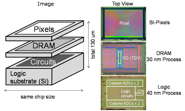

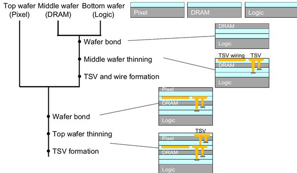
The logic substrate has 6 layers. It would include 5 copper layers and 1 aluminum layer. The DRAM has 3 aluminum layers. The topmost BI pixels layer 5 copper layers and 1 aluminum. After fabricating the three layers, DRAM is flipped to face the chip, and then it is thinned to measure 3 microns.
The two layers are connected through the use of wiring and TSVs. Once that is completed, the pixel wafer is flipped onto the above combination. The backside of the pixel wafer is also thinned. You can find the construction from the following image.

Sony could reduce the I/O area and power consumption through the above design. One of the best aspects that this design brought ahead is the same thickness as on the conventional 2-layer pixel/logic CIS stacked chips.
It has also been made clear that the configuration was tested under different platforms.
The Commercial availability of 3-Layer Stacked CMOS Image Sensor
The commercial product or chip does provide you access to an enhanced degree of improvement and the same capability as observed on the one showcased at the event. The cross-section of the CIS indicated the following idea
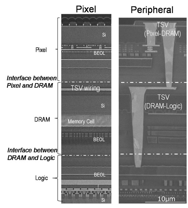

You can see the different layers and how they have been placed. You should also see the TSV wiring for the power and ground rails.
As we found as the commercialized version, the final chip had the following measurements – 19.3M pixels of 1.22 x 1.22 μm each and a 1 Gbit DRAM. Even the TSVs that Sony used had 2.5 μm and a pitch of 6.3 μm with a line of 2 μm and space of 0.64 μm.
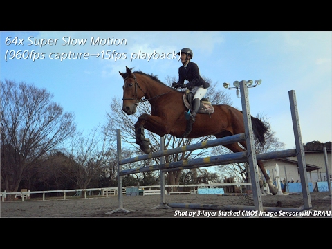
We found the chip offering a very decent experience in terms of performance. It was found to come with 120 fps for all 19.3M pixels and can produce 960 fps FHD (1,920 x 1,080) super slow-motion video.
The following video should provide you a great idea of how does the new CMOS image sensor offer you –
The specifications of the new sensor
The spec sheet for the sensor would include
| Effective pixel count | 5520 (H) x 3840 (V) 21.2 megapixels |
| Image size | Diagonal 7.73mm (Type 1/2.3) |
| Unit cell size | 1.22μm (H) x 1.22μm (V) |
| Frame rate (for images( | 30fps
4:3 19.3 megapixels / 16:9 17.1 megapixels |
| Frame rate for videos | 60fps
4K (3840 x 2160) 240fps Full HD / 720p |
| Reading speed | 8.478 ms (4:3 19.3 megapixels) / 6.962 ms (16:9 17.1 megapixels) |
| Power supply | 2.5V / 1.8V / 1.1V |
| Image format | Bayer RAW |
| Output | MIPI (CSI2) D-PHY 2.2Gbps/lane / C-PHY 2.0Gsps/lane |
| DRAM capacity | 1G bit |
The Concluding Thoughts
Sony came up with the development results of the all-new sensor at the International Solid-State Circuits Conference (ISSCC) in San Francisco in 2017. It even claimed that the new sensor came up with a performance that was eight times better than the Sony IMX318.